Impact of Crystal Size, P-layer and Doping Rate on the Intrinsic Loss Rate Imposed by Shunt Resistance in the Depletion Zone and on the Rear Surface Loss Rate
Improving the performance of photovoltaic cells requires optimization of the design stages through crystallization and the percentage of impurities introduced into the n+ layer and the p layer. Doping is crucial for solar cells because it creates a transition zone, an essential structure for converting light into electricity. This process modifies the properties of crystals by adding impurities to create two zones, one with an excess of electrons (n-type) and the other with an excess of holes (p-type). This difference in charge creates an electric field that forces the electrons and holes to separate and move in opposite directions, enabling the generation of a useful electric current. However, these electrons and holes recombine at the surfaces, limiting the efficiency of the photovoltaic cell. The objective is to find a solution to reduce surface losses by studying the impact of polycrystalline crystal dimensions and the effect of the p-layer on the effect of the impurity rate of said layer on the intrinsic carrier loss rate imposed by the shunt resistance in the depletion zone and on the carrier loss rate at the rear surface. This study has made it possible to establish the mathematical expressions needed to better understand the influence of surface recombination rates. These mathematical expressions link the intrinsic loss rate in the depletion zone and the carrier loss rate at the rear surface to the impurity rate of the p-layer, the crystal dimensions and the thickness of the p-layer. The simulation results show that: if the doping concentration of the p-layer (Nb) is between 3.1015 and 1018 cm-3, the intrinsic loss rate due to shunt resistance in the depletion region and the loss rate at the rear surface decrease rapidly as the impurity concentration of the p-layer (Nb) increases. Below and beyond this interval, Intrinsic loss rate imposed by the shunt resistance in the depletion zone and loss rate at the rear surface are independent of the impurity level of the p-layer. This range of doping concentrations varies with crystal size and the thickness of the p-layer. The intrinsic loss rate imposed by the shunt resistance in the depletion region decreases when the crystals are small and the p-layer is thin, while it increases when the crystals are large. As for Sb loss rate at the rear surface., it decreases with crystal size but increases with layer height p.
This is an Open Access article, distributed under the terms of the Creative Commons Attribution 4.0 International License (http://creativecommons.org/licenses/by/4.0/), which permits unrestricted use, distribution and reproduction in any medium or format, provided the original work is properly cited.
Intrinsic Loss Rate, Back-side Loss Rate, Shunt Resistance, Doping Rate, Crystal Size, P Layer
1. Introduction
The performance of solar cells is mainly characterized by their efficiency, which is generally between 10 and 20% for current models. This performance depends on several factors, including: the material used (such as polycrystalline silicon), the type of technology, intrinsic material parameters such as the thickness of the P layer
[1]
M. Camara, M. Thiame, I. Faye, S. Traore, M. B. Mouta, B. Fickou, L. Diatta, Influence of Crystal Dimensions and P-Layer Thickness on the Optimum Doping Rate for the Best Diffusion Capacity of a Polycrystalline Solar Cell, Journal of Materials Science and Chemical Engineering, 13(9): (2025) 55-66
M. Camara, M. Toure, H. Siba, H. Ch. Diallo, O. F. Camara, M. Thiame, Impact of Polycrystalline Crystal Size and the Capture Effect at the Contact Surface of Two Crystals on the Effect of P-layer Dopant on Some Electrical Parameters International Journal of Sustainable and Green Energy 2025, Vol. 14, No. 3: (2025) 211-217
M. S. Diop, H. Y. Ba, Nd. Thiam, I. Diatta, Y. Traore, M. L. Ba, El. Sow, O. Mballo, Gregoire. Sissoko Surface Recombination concept as applied to determinate silicon solar cell base optimum thickness with doping level effect. World Journal of Condensed Matter Physics, 9, (2019) 102-111
M. Camara, M. Toure, H. Siba, M. B. Mouta, O. F. Camara and M. Thiame Analyse of Impact of Temperature, Grain Size and Magnetic Field on Effective Diffusion Length, Asian Journal of Science and Technology Vol. 16, Issue, 02: (2025) 13516-13519,
R. Mats, B. Henry, M. Mans and N. r Edvard. A Novel Tehcnical for the Simultaneous Measurement of Ambipolar Carrier Lifetime and Diffusion Coefficient in Silicon. Solid-State Electronics Volume 35, Issue 9, September (1992) 1223-1227,
K. Misiakos, C. H. Wang, A. Neugroschel and F. A. Lindholm Similtaneous extraction of minoritycarrier parameters in crystalline semiconductors by lateral photocurren, J. Appl. Phys. 67(1): (1990) 321-333.
Rugider M., Puzzer T., Schäffer E., Warta W., Glunz S. W., Würfel P., Trupke T. Diffusion lengths of silicon solar cells frop luminescence images. 22nd European Photovoltaic Solar Energy Conferences. 3-7: (2007) 309,
M. Thiame, A. Diene, B. Seibou, Ch. T. Sarr, M. L. O. Cheikh, I. Diatta, M. Dieye, Y. Traore, G. Sissoko, 3D Study of a Bifacial Polycrystalline Silicon Solar Cell Back Surface Illuminated: Influence of Grain Size and Recombination Velocity, JSER. 4(1): (2017) 135-145.
[9]
Mbao O., Thiame M., LY I., Datta I., Diouf M. S., Traore Y., Ndiaye M. and Sissoko G., 3D Study of a Polycrystalline Bifacial Silicon Solar Cell, Illuminated Simultaneously by Both Sides: Grain Size and Recombination Velocity Influence. International Journal of Innovative Science, Engineering & Technology, Vol. 3 Issue 12: (2016), pp. 152-162
L. H. Diallo., M. A. Saidou., Wereme A., Sissoko G., New Approach of Both Junction and Back Surface Recombination Velocity in a 3D Modelling Study of a Polycrystalline Silicon Solar Cell. Eur. Phys. J. Appl. Phys. 42: (2008) 203-211,
Rugider M., Puzzer T., Schäffer E., Warta W., Glunz S. W., Würfel P., Trupke T. Diffusion lengths of silicon solar cells frop luminescence images. 22nd European Photovoltaic Solar Energy Conferences. 3-7: (2007) 309,
M. Thiame, A. Diene, B. Seibou, Ch. T. Sarr, M. L. O. Cheikh, I. Diatta, M. Dieye, Y. Traore, G. Sissoko, 3D Study of a Bifacial Polycrystalline Silicon Solar Cell Back Surface Illuminated: Influence of Grain Size and Recombination Velocity, JSER. 4(1): (2017) 135-145.
[9]
Mbao O., Thiame M., LY I., Datta I., Diouf M. S., Traore Y., Ndiaye M. and Sissoko G., 3D Study of a Polycrystalline Bifacial Silicon Solar Cell, Illuminated Simultaneously by Both Sides: Grain Size and Recombination Velocity Influence. International Journal of Innovative Science, Engineering & Technology, Vol. 3 Issue 12: (2016), pp. 152-162
Diasse O., Diao A., Wade M., Diouf M. S., Diatta I., Mane R., Traore Y., and Sissoko G., Back Surface Recombination Velocity Modeling in White Biased Silicon Solar Cell Under Steady State. J. Mod. Phys. 9: (2018) 189-201
Rugider M., Puzzer T., Schäffer E., Warta W., Glunz S. W., Würfel P., Trupke T. Diffusion lengths of silicon solar cells frop luminescence images. 22nd European Photovoltaic Solar Energy Conferences. 3-7: (2007) 309,
M. Thiame, A. Diene, B. Seibou, Ch. T. Sarr, M. L. O. Cheikh, I. Diatta, M. Dieye, Y. Traore, G. Sissoko, 3D Study of a Bifacial Polycrystalline Silicon Solar Cell Back Surface Illuminated: Influence of Grain Size and Recombination Velocity, JSER. 4(1): (2017) 135-145.
[9]
Mbao O., Thiame M., LY I., Datta I., Diouf M. S., Traore Y., Ndiaye M. and Sissoko G., 3D Study of a Polycrystalline Bifacial Silicon Solar Cell, Illuminated Simultaneously by Both Sides: Grain Size and Recombination Velocity Influence. International Journal of Innovative Science, Engineering & Technology, Vol. 3 Issue 12: (2016), pp. 152-162
, the technology used for their manufacture and the conditions of use, with notable advances such as the use of bifacial photovoltaic cells that can increase power output.
Recombination in photovoltaic cells are processes in which electron-hole pairs created by light absorption come together and neutralize each other before contributing to the production of an electric current. This recombination, which can occur both within the bulk of the material (base) and at the surfaces, represent performance losses for the solar cell, hence the importance of studying their loss rate and seeking to reduce them.
Previously, some researchers have exploited surface recombination velocities to optimize the thickness of the p-layer using one-dimensional models
[12]
M. Thiame, M. Camara, M. L. Cheikh, S. Gueye, O. Sow, My. Wade and G. Sissoko, Study of a Bifacial Silicon Photovoltaic Cell in Steady State Subjected to a Magnetic Field Under Monochromatic Illumination from the Rear Surface: Determination of the Optimal Base Thickness, Int. J. Adv. Res. 11(06): (1992) 889–901,, Int. J. Adv. Res. 11(06): (1992) 889-901,
. The aim of this work is to contribute to existing research on the behavior of polycrystalline silicon photovoltaic cells under the impact of crystal dimensions on the effect of the impurity rate of the p-layer on the intrinsic loss rate imposed by the shunt resistance in the junction and on the electron loss rate on the rear surface of three-dimensional models.
It is based on the study of the x and y dimensions of the crystal, the height of the p-layer and the doping level of the p-layer on surface loss velocities. The doping level that reduces the loss velocity at the surfaces limiting the p-layer is given under the influence of the crystal dimensions and the height of the p-layer.
2. Model and Assumptions
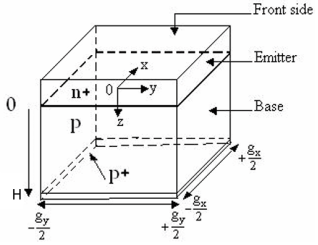
The polycrystalline silicon photovoltaic cell used is an n+-p-p+ structure under constant polychromatic light. We have chosen a columnar model.
[13]
J. Dugas, Solar Energy Materials and Solar Cells 32, 1 (1994) 71-88
Figure 1. The columnar geometry of a crystal used as a model.
We have made the following assumptions:
1) The Crystal have a square cross-section (gx = gy = g; 7.3 µm ⩽ g ⩽ 120 µm) and their electrical properties are homogeneous. Therefore, we can work in the Cartesian coordinate system.;
2) The study will be limited to illuminating the front panel only;
3) the light is uniform, the creation rate depends solely on the depth z of layer p, because the distribution is uniform along x and y;
4) the side of layer n+ receiving light is coated with an anti-reflective coating to increase light absorption
[14]
H. S. Rauschenbach, Solar Cell Array Design Handbook. The Principles and Technology of Photovoltaic Energy Conversion (Van Nostrand Reinhold Ltd., New York): 564.
[14]
;
5) The crystal junction and the n+/p transition zone are orthogonal, and their recombination rates are independent of the creation rate under AM1.5 illuminations. Thus, the boundary conditions of the continuity equation are linear;
6) the contribution of the n+ layer and the depletion zone is neglected
[13]
J. Dugas, Solar Energy Materials and Solar Cells 32, 1 (1994) 71-88
, so this analysis is only developed in the region of the p layer.
Continuity equation for photogenerated minority carriers in the three-dimensional p-layer is:
(1)
Dn (Nb) and Ln (Nb) are respectively the diffusion constant and the diffusion length of carriers through the n+/p interface; they depend on the doping concentration of the p layer according to the equations below:
(2)
(3)
With the lifetime of electrons within the p-layer, which depends on the impurity concentration according to the equation (4).
(4)
Nb is the impurity concentration of the p-layer.
G (z) the carrier creation rate depends on the position in the p-layer and can be written as follows
[15]
H. El Ghitani, S. Martinuzzi, J. Appl. Phys. 66, 4, 1989 1717-1722
G. Sissoko, E. Nanema, A. Correa, M. Adj, A. L. Ndiaye, M. N. Diarra, Proceedings of World Renewable Energy Conference, Florence-Italy, (1998) 1856-1859.
[13, 17]
:
(6)
Where Ck and Cj are obtained from the following x and y limits of the crystal:
(7)
(8)
Equations (7) and (8) define a recombination velocity at the boundaries of the Sgb crystal that reflects the flow of carriers lost through the crystal joints, where gx and gy are the sizes of the crystals along the x and y axes. By replacing δ (x,y,z) with its expression in the two boundary conditions above, we obtain the following transcendental equations:
(9)
(10)
Ck and Cj are the actual values of the intra-crystal surface loss velocity. By substituting δ (x,y,z) into the continuity equation and using the fact that cosine functions are orthogonal, we obtain the following differential equation:
(11)
Where
(12)
and
(13)
may be written in the form:
(14)
With
(15)
The constants Nk,j and Ok,j are calculated by vocalizing on the limits following z of layer p:
At the interface n+/p (z=0):
(16)
At z=H:
(17)
3. Photoelectric Current Density
The photocurrent density of photovoltaic cells is obtained by solving the equation (18):
(18)
Where q is the charge of the electron.
(19)
With
(20)
4. Intrinsic Loss Rate of the Crystal Imposed by the Shunt Resistance in the Depletion Zone
Equation (16) defines the manner in which minority electrons are lost at the n+/p interface (Sf). Sf appears as an effective characteristic of the depletion zone and is related to parameters specific to the crystal (crystal size, doping rate of the p-layer, thickness of the p-layer, etc.) and to the state of the depletion zone (with or without polarization). Sf provides information on the number of carriers that cross the depleted zone. It defines the depletion zone as an active zone
[17]
G. Sissoko, E. Nanema, A. Correa, M. Adj, A. L. Ndiaye, M. N. Diarra, Proceedings of World Renewable Energy Conference, Florence-Italy, (1998) 1856-1859.
[18]
B. Ba, M. Kane, A. Fickou, G. Sissoko, Solar Energy Materials and Solar Cells 31, 1 Volume 39, Issue 1: (1995) 71-81,
. When it decreases to zero, the current flowing through the depletion zone is cancelled out, so that the electrons and holes remain blocked on either side of the depletion zone: open circuit state for an ideal photovoltaic cell. For a photovoltaic cell that is not ideal (a case that reflects reality with losses in the depletion zone), a weak current flows through the depletion zone, indicating the presence of an internal charge within the crystal: this is the shunt resistance (Rsh) of the photovoltaic cell. This shunt resistance induces a loss rate specific to the crystal in the depletion zone (Sf0)
[18]
B. Ba, M. Kane, A. Fickou, G. Sissoko, Solar Energy Materials and Solar Cells 31, 1 Volume 39, Issue 1: (1995) 71-81,
A. Rohatgi, S. Narasimha, D. S. Ruby, Proceedings of the 2nd World Conference and Exhibition on Photovoltaic Solar Energy Conversion (Stephens, Bedford): (998) 1566-1569,
[18, 19]
, which depends solely on parameters specific to the photovoltaic cell crystal. Thus, Sf is the combination of two contributions: Sf0, which is the intrinsic part imposed by the shunt resistance, and Sfj, which provides information on the current density imposed by an external load. Sf defines the operating points of the photovoltaic cell: Sf = Sfj + Sf0
[20]
F. I. Barro, I. Zerbo, O. H. Lemrabott, F. Zougmore, G. Sissoko (2001) Proceedings of the 17th European Photovoltaic Solar Energy Conference and Exhibition, Munich, Germany (2001) 368-371.
[20]
. In this section, we focus on the intrinsic loss rate imposed by the shunt resistance in the depletion zone (Sf0 (cm/s)). It depends on the dimensions of the crystals, the loss velocity at the crystal boundaries Sgb, the actual value of the loss velocity at the intra-crystal surface
[12]
M. Thiame, M. Camara, M. L. Cheikh, S. Gueye, O. Sow, My. Wade and G. Sissoko, Study of a Bifacial Silicon Photovoltaic Cell in Steady State Subjected to a Magnetic Field Under Monochromatic Illumination from the Rear Surface: Determination of the Optimal Base Thickness, Int. J. Adv. Res. 11(06): (1992) 889–901,, Int. J. Adv. Res. 11(06): (1992) 889-901,
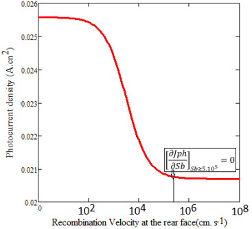
Figure 2. Photoelectric current profile as a function of rear surface loss rate.
According to the photoelectric current profile as a function of the recombination rate at the rear surface (Figure 2) and for high values of Sb
[21]
G. Sissoko, C. Museruka, A. Corr´ea, I. Gaye, A. L. Ndiaye, Proceedings of the 4th World Renewable Energy Congress, Denver, Colorado: (1996) 1487-1490.
[21]
Figure 2, the photocurrent density remains constant for values of Sb ≥ 7.105 cm/s. This allowed us to write:
(21)
Solving equation (21) leads to analytical expressions for the intrinsic loss rate in the depletion zone Sf0:
(22)
5. Rear Surface Loss Rate
Equation (17) defines the concept of carrier loss rate at the rear surface. Sb quantify the rate at which excess minority carriers photo created in the P layer are lost at the rear of the photovoltaic cell
[21]
G. Sissoko, C. Museruka, A. Corr´ea, I. Gaye, A. L. Ndiaye, Proceedings of the 4th World Renewable Energy Congress, Denver, Colorado: (1996) 1487-1490.
[22]
S. M. Sze, Physics of semiconductor Devices, 2nd edn. (Wiley Interscience, New York,), Wiley, 30 sept. (1981) 868.
[21, 22]
. Sb (cm/s) is related to the dimensions of the crystals along x and y, to the loss rate at the crystal boundaries Sgb, to the actual value of the carrier loss rate at the intra-crystal surface
[21]
G. Sissoko, C. Museruka, A. Corr´ea, I. Gaye, A. L. Ndiaye, Proceedings of the 4th World Renewable Energy Congress, Denver, Colorado: (1996) 1487-1490.
[22]
S. M. Sze, Physics of semiconductor Devices, 2nd edn. (Wiley Interscience, New York,), Wiley, 30 sept. (1981) 868.
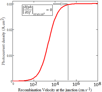
Figure 3. Photoelectric current profile as a function of junction loss rate.
Based on the photocurrent curve as a function of Sf Figure 3, and for high Sf values, the photocurrent exhibits a horizontal plateau Figure 3, which allowed us to write equation (23):
(23)
Equation (23) leads to analytical expressions for the electron loss rate at the rear surface Sb.
(24)
6. Impact of Crystal Size on the Effect of Doping on the Intrinsic Loss Rate Imposed by Shunt Ressistan
Sfo (cm/s) depends heavily on diffusion parameters
[21]
G. Sissoko, C. Museruka, A. Corr´ea, I. Gaye, A. L. Ndiaye, Proceedings of the 4th World Renewable Energy Congress, Denver, Colorado: (1996) 1487-1490.
[22]
S. M. Sze, Physics of semiconductor Devices, 2nd edn. (Wiley Interscience, New York,), Wiley, 30 sept. (1981) 868.
[21, 22]
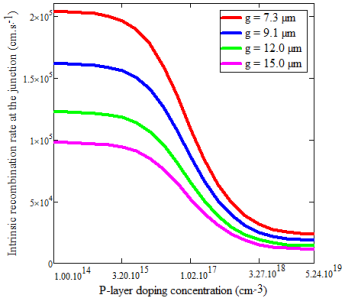
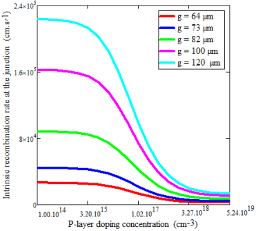
but also on the percentage of impurity introduced into the P layer and the size of the crystals. Figures 4 and 5 show Sf0 as a function of the doping percentage of the P layer for small and large crystals. For this, we set Sgb = 103 cm.s-1, H = 200 μm. These values are fixed based on a preliminary study that allowed us to obtain the optimal values for these parameters.
Analysis of the impact of the doping percentage of the p-layer on the intrinsic loss rate (Sf0 (cm/s)) shows three zones. Figures 4 and 5:
Zone I: , Sf0 varies almost not at all with the doping percentage of the p-layer. Consequently, the impact of the doping percentage of the p-layer only becomes significant above the critical threshold Nb = 3.1015 cm⁻³, marking the start of the improvement in the conductivity of polycrystalline silicon materials, which depends heavily on the interaction between the impurity percentage of the p-layer, the height of the p-layer, and the size of the crystals. We also note that this threshold shifts numerically as the size of small crystals increases Figure 4, while we observe the opposite when the size of large crystals increases Figure 5.
Figure 5. Intrinsic electron loss rate as a function of the doping percentage of the p-layer for large crystal sizes.
Zone II: , Sf0 decreases rapidly with the doping percentage of the p-layer. To produce crystals with high potentials by reducing intrinsic carrier losses imposed by shunt resistance, it is preferable to maintain the dopant concentration of the p-layer within this range. An increase in doping within this range reduces the defect density in the solar cell. Fewer defects mean fewer recombination sites, which reduces leakage currents, series resistance, intrinsic recombination rate and increases shunt resistance Figure 5.
Zone III: , reflecting the system's inability to keep up with rapid changes in the doping level of the P layer. This is because in heavily doped crystals, the mechanism linked to the deformation of energy band boundaries causes the growth of tails that enter the space separating the valence band from the conduction band. The energy levels of these impurities combine to form an impurity band that crosses the valence band, leading to a modification of the crystal lattice. These modifications lead to a decrease in the width of the crystal's band gap. As a result, the crystal loses its semiconductor properties and becomes a conductor.
We also note that increasing the dimensions along x and y of small crystals increases the intrinsic loss rate Figure 4, while increasing the dimensions of large crystals decreases it Figure 5. Crystal size has an indirect effect on the intrinsic loss rate in the transition zone, mainly by impacting the defect density and the distance that charge carriers must travel. In addition, smaller crystals may have a larger relative surface area, which increases the intrinsic recombination rate Figure 4. Slower crystal growth results in larger crystals with lower defect density and smaller relative surface area, which can reduce the intrinsic recombination rate imposed by shunt resistance Figure 5.
7. Impact of Crystal Size on the Effect of Impurity Percentage on Rear Surface Loss Rate
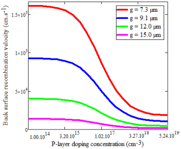
In this section, we present in Figure 6 the electron loss rate at the rear surface Sb as a function of the dopant percentage of the p-layer for several crystal sizes.
The evolution of Sb at the rear face is obtained for a recombination rate at the crystal joints set at 103 cm-3 after conducting a study to obtain its optimal value and for a p-layer thickness set at 200 μm.
Figure 6. Back-surface recombination velocity as a function of P-layer doping concentration for different crystal sizes.
As previously mentioned in the paragraph above, analysis of the impact of the doping percentage of the P layer on the rear surface loss rate (Sb (cm/s)) shows three areas in Figure 6:
Zone I: , Sb varies very little with the doping level of the P layer. Consequently, the influence of the doping percentage of the P layer only becomes significant above the critical threshold Nb = 3.1015 cm-3, marking the start of the improvement in the conductivity of polycrystalline silicon materials. We also note that this threshold shifts numerically as the crystal size increases Figure 6.
Zone II: , Sb decreases considerably with the percentage of impurities in the p-layer. To produce high-performance crystals by reducing the rate of carrier loss (electrons and holes) due to recombination at the rear surface of the solar cell, we recommend maintaining the impurity concentration within this range Figure 6.
Zone III: , reflecting the system's inability to keep up with rapid variations in the doping level of the P layer. This is because, in heavily doped crystals, the mechanisms involved in modifying the energy band boundaries cause deformation of the crystal lattice. As a result, polycrystalline silicon loses its semiconductor properties and becomes a conductor Figure 6.
We also observe that when small crystals tend towards large ones, there is a decrease in carrier loss at the rear surface. Figure 6 This is because rear surface losses are mainly influenced by surface quality and boundary conditions. Small crystals can create grain boundaries that become traps for charge carriers, thereby increasing recombination at the surface. This explains the decrease in carrier losses at the rear surface when the crystal size is increased Figure 6.
8. Impact of the Thickness of P Layer on the Intrinsic Loss Rate Imposed by the Shunt Resistance
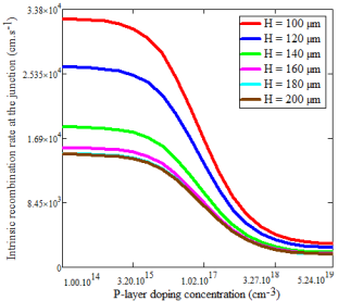
Figure 7. Intrinsic loss rate as a function of the dopant concentration of the p-layer for different p-layer heights.
Here we study the effect of the height of the p layer on the doping concentration of the P layer on the intrinsic loss rate imposed by the shunt resistance.
In Figure 7, we analyze a decrease in the intrinsic loss rate imposed by the shunt resistance with an increase in the height of the P-layer of the photovoltaic cell. The height of the P-layer directly influences recombination at the depletion zone. A thicker P layer reduces recombination because it increases the distance that carriers must travel to reach the space charge region, which increases the probability of their recombination within the volume of the P layer rather than at the surface. However, an excessively large P layer can reduce efficiency because fewer carriers are generated near the transition region.
9. Impact of P Layer Thickness on the Effect of Dopant Concentration on Back Surface Loss Rate
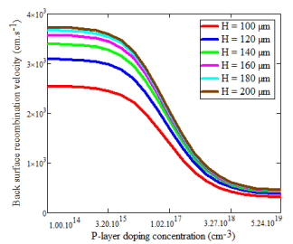
Figure 8. Back-side loss rate as a function of the dopant concentration of the P layer for different thicknesses of the P layer.
Figure 8 shows the evolution of rear surface losses Sb as a function of impurity introduced into P layer for several thicknesses of P layer.
This evolution of rear surface losses Sb is obtained for a fixed crystal size (g = 15 µm) and a fixed joint loss rate. (Sgb = 103 cm/s).
We note in Figure 8 that, contrary to the effect of the thickness of the P layer on the intrinsic loss rate, the increase in the height of the P layer increases carrier losses at the rear surface. This is because the thicker the P layer, the greater the distance that charge carriers must travel, thereby increasing the probability of recombination and reducing the efficiency of the solar cell. To minimize rear losses, surface treatment processes (such as passivation) are used to reduce the recombination rate, or solar cells are designed with a thinner P-layer so that the carriers quickly reach the transition zone before recombining.
10. Conclusion
In this study, we focus on a multicrystalline silicon photovoltaic cell and analyze the effect of crystal dimensions on the impact of impurity concentration in the p-layer on recombination rates at the surfaces bordering the p-layer. The aim is to reduce surface losses in multicrystalline silicon photovoltaic cells.
For , The recombination rates at the surfaces limiting the P layer of the photovoltaic cell decrease significantly with increasing impurity concentration in the P layer. This interval is influenced by the crystal size and the thickness of the P layer.
Analysis of the effect of crystal dimensions reveals that small crystals reduce recombination in the depletion zone and on the rear surface, while large crystals cause an increase in intrinsic losses in the transition zone.
As for the thickness of layer P, its elevation causes a decrease in recombination in the transition zone, while increasing the rate of losses at the rear surface.
M. Camara, M. Thiame, I. Faye, S. Traore, M. B. Mouta, B. Fickou, L. Diatta, Influence of Crystal Dimensions and P-Layer Thickness on the Optimum Doping Rate for the Best Diffusion Capacity of a Polycrystalline Solar Cell, Journal of Materials Science and Chemical Engineering, 13(9): (2025) 55-66
M. Camara, M. Toure, H. Siba, H. Ch. Diallo, O. F. Camara, M. Thiame, Impact of Polycrystalline Crystal Size and the Capture Effect at the Contact Surface of Two Crystals on the Effect of P-layer Dopant on Some Electrical Parameters International Journal of Sustainable and Green Energy 2025, Vol. 14, No. 3: (2025) 211-217
M. S. Diop, H. Y. Ba, Nd. Thiam, I. Diatta, Y. Traore, M. L. Ba, El. Sow, O. Mballo, Gregoire. Sissoko Surface Recombination concept as applied to determinate silicon solar cell base optimum thickness with doping level effect. World Journal of Condensed Matter Physics, 9, (2019) 102-111
M. Camara, M. Toure, H. Siba, M. B. Mouta, O. F. Camara and M. Thiame Analyse of Impact of Temperature, Grain Size and Magnetic Field on Effective Diffusion Length, Asian Journal of Science and Technology Vol. 16, Issue, 02: (2025) 13516-13519,
R. Mats, B. Henry, M. Mans and N. r Edvard. A Novel Tehcnical for the Simultaneous Measurement of Ambipolar Carrier Lifetime and Diffusion Coefficient in Silicon. Solid-State Electronics Volume 35, Issue 9, September (1992) 1223-1227,
K. Misiakos, C. H. Wang, A. Neugroschel and F. A. Lindholm Similtaneous extraction of minoritycarrier parameters in crystalline semiconductors by lateral photocurren, J. Appl. Phys. 67(1): (1990) 321-333.
Rugider M., Puzzer T., Schäffer E., Warta W., Glunz S. W., Würfel P., Trupke T. Diffusion lengths of silicon solar cells frop luminescence images. 22nd European Photovoltaic Solar Energy Conferences. 3-7: (2007) 309,
M. Thiame, A. Diene, B. Seibou, Ch. T. Sarr, M. L. O. Cheikh, I. Diatta, M. Dieye, Y. Traore, G. Sissoko, 3D Study of a Bifacial Polycrystalline Silicon Solar Cell Back Surface Illuminated: Influence of Grain Size and Recombination Velocity, JSER. 4(1): (2017) 135-145.
[9]
Mbao O., Thiame M., LY I., Datta I., Diouf M. S., Traore Y., Ndiaye M. and Sissoko G., 3D Study of a Polycrystalline Bifacial Silicon Solar Cell, Illuminated Simultaneously by Both Sides: Grain Size and Recombination Velocity Influence. International Journal of Innovative Science, Engineering & Technology, Vol. 3 Issue 12: (2016), pp. 152-162
L. H. Diallo., M. A. Saidou., Wereme A., Sissoko G., New Approach of Both Junction and Back Surface Recombination Velocity in a 3D Modelling Study of a Polycrystalline Silicon Solar Cell. Eur. Phys. J. Appl. Phys. 42: (2008) 203-211,
Diasse O., Diao A., Wade M., Diouf M. S., Diatta I., Mane R., Traore Y., and Sissoko G., Back Surface Recombination Velocity Modeling in White Biased Silicon Solar Cell Under Steady State. J. Mod. Phys. 9: (2018) 189-201
M. Thiame, M. Camara, M. L. Cheikh, S. Gueye, O. Sow, My. Wade and G. Sissoko, Study of a Bifacial Silicon Photovoltaic Cell in Steady State Subjected to a Magnetic Field Under Monochromatic Illumination from the Rear Surface: Determination of the Optimal Base Thickness, Int. J. Adv. Res. 11(06): (1992) 889–901,, Int. J. Adv. Res. 11(06): (1992) 889-901,
H. S. Rauschenbach, Solar Cell Array Design Handbook. The Principles and Technology of Photovoltaic Energy Conversion (Van Nostrand Reinhold Ltd., New York): 564.
[15]
H. El Ghitani, S. Martinuzzi, J. Appl. Phys. 66, 4, 1989 1717-1722
G. Sissoko, E. Nanema, A. Correa, M. Adj, A. L. Ndiaye, M. N. Diarra, Proceedings of World Renewable Energy Conference, Florence-Italy, (1998) 1856-1859.
[18]
B. Ba, M. Kane, A. Fickou, G. Sissoko, Solar Energy Materials and Solar Cells 31, 1 Volume 39, Issue 1: (1995) 71-81,
A. Rohatgi, S. Narasimha, D. S. Ruby, Proceedings of the 2nd World Conference and Exhibition on Photovoltaic Solar Energy Conversion (Stephens, Bedford): (998) 1566-1569,
[20]
F. I. Barro, I. Zerbo, O. H. Lemrabott, F. Zougmore, G. Sissoko (2001) Proceedings of the 17th European Photovoltaic Solar Energy Conference and Exhibition, Munich, Germany (2001) 368-371.
[21]
G. Sissoko, C. Museruka, A. Corr´ea, I. Gaye, A. L. Ndiaye, Proceedings of the 4th World Renewable Energy Congress, Denver, Colorado: (1996) 1487-1490.
[22]
S. M. Sze, Physics of semiconductor Devices, 2nd edn. (Wiley Interscience, New York,), Wiley, 30 sept. (1981) 868.
Camara, M., Conde, D., Toure, M., Yansane, I. S., Camara, O. F., et al. (2026). Impact of Crystal Size, P-layer and Doping Rate on the Intrinsic Loss Rate Imposed by Shunt Resistance in the Depletion Zone and on the Rear Surface Loss Rate. International Journal of Materials Science and Applications, 15(4), 143-152. https://doi.org/10.11648/j.ijmsa.20261504.12
Camara, M.; Conde, D.; Toure, M.; Yansane, I. S.; Camara, O. F., et al. Impact of Crystal Size, P-layer and Doping Rate on the Intrinsic Loss Rate Imposed by Shunt Resistance in the Depletion Zone and on the Rear Surface Loss Rate. Int. J. Mater. Sci. Appl.2026, 15(4), 143-152. doi: 10.11648/j.ijmsa.20261504.12
Camara M, Conde D, Toure M, Yansane IS, Camara OF, et al. Impact of Crystal Size, P-layer and Doping Rate on the Intrinsic Loss Rate Imposed by Shunt Resistance in the Depletion Zone and on the Rear Surface Loss Rate. Int J Mater Sci Appl. 2026;15(4):143-152. doi: 10.11648/j.ijmsa.20261504.12
@article{10.11648/j.ijmsa.20261504.12,
  author = {Moussa Camara and Djime Conde and Mamoudou Toure and Ibrahima Sory Yansane and Ousmane Fanta Camara and Moustapha Thiame},
  title = {Impact of Crystal Size, P-layer and Doping Rate on the Intrinsic Loss Rate Imposed by Shunt Resistance in the Depletion Zone and on the Rear Surface Loss Rate},
  journal = {International Journal of Materials Science and Applications},
  volume = {15},
  number = {4},
  pages = {143-152},
  doi = {10.11648/j.ijmsa.20261504.12},
  url = {https://doi.org/10.11648/j.ijmsa.20261504.12},
  eprint = {https://article.sciencepublishinggroup.com/pdf/10.11648.j.ijmsa.20261504.12},
  abstract = {Improving the performance of photovoltaic cells requires optimization of the design stages through crystallization and the percentage of impurities introduced into the n+ layer and the p layer. Doping is crucial for solar cells because it creates a transition zone, an essential structure for converting light into electricity. This process modifies the properties of crystals by adding impurities to create two zones, one with an excess of electrons (n-type) and the other with an excess of holes (p-type). This difference in charge creates an electric field that forces the electrons and holes to separate and move in opposite directions, enabling the generation of a useful electric current. However, these electrons and holes recombine at the surfaces, limiting the efficiency of the photovoltaic cell. The objective is to find a solution to reduce surface losses by studying the impact of polycrystalline crystal dimensions and the effect of the p-layer on the effect of the impurity rate of said layer on the intrinsic carrier loss rate imposed by the shunt resistance in the depletion zone and on the carrier loss rate at the rear surface. This study has made it possible to establish the mathematical expressions needed to better understand the influence of surface recombination rates. These mathematical expressions link the intrinsic loss rate in the depletion zone and the carrier loss rate at the rear surface to the impurity rate of the p-layer, the crystal dimensions and the thickness of the p-layer. The simulation results show that: if the doping concentration of the p-layer (Nb) is between 3.1015 and 1018 cm-3, the intrinsic loss rate due to shunt resistance in the depletion region and the loss rate at the rear surface decrease rapidly as the impurity concentration of the p-layer (Nb) increases. Below and beyond this interval, Intrinsic loss rate imposed by the shunt resistance in the depletion zone and loss rate at the rear surface are independent of the impurity level of the p-layer. This range of doping concentrations varies with crystal size and the thickness of the p-layer. The intrinsic loss rate imposed by the shunt resistance in the depletion region decreases when the crystals are small and the p-layer is thin, while it increases when the crystals are large. As for Sb loss rate at the rear surface., it decreases with crystal size but increases with layer height p.},
 year = {2026}
}
TY  - JOUR
T1  - Impact of Crystal Size, P-layer and Doping Rate on the Intrinsic Loss Rate Imposed by Shunt Resistance in the Depletion Zone and on the Rear Surface Loss Rate
AU  - Moussa Camara
AU  - Djime Conde
AU  - Mamoudou Toure
AU  - Ibrahima Sory Yansane
AU  - Ousmane Fanta Camara
AU  - Moustapha Thiame
Y1  - 2026/07/08
PY  - 2026
N1  - https://doi.org/10.11648/j.ijmsa.20261504.12
DO  - 10.11648/j.ijmsa.20261504.12
T2  - International Journal of Materials Science and Applications
JF  - International Journal of Materials Science and Applications
JO  - International Journal of Materials Science and Applications
SP  - 143
EP  - 152
PB  - Science Publishing Group
SN  - 2327-2643
UR  - https://doi.org/10.11648/j.ijmsa.20261504.12
AB  - Improving the performance of photovoltaic cells requires optimization of the design stages through crystallization and the percentage of impurities introduced into the n+ layer and the p layer. Doping is crucial for solar cells because it creates a transition zone, an essential structure for converting light into electricity. This process modifies the properties of crystals by adding impurities to create two zones, one with an excess of electrons (n-type) and the other with an excess of holes (p-type). This difference in charge creates an electric field that forces the electrons and holes to separate and move in opposite directions, enabling the generation of a useful electric current. However, these electrons and holes recombine at the surfaces, limiting the efficiency of the photovoltaic cell. The objective is to find a solution to reduce surface losses by studying the impact of polycrystalline crystal dimensions and the effect of the p-layer on the effect of the impurity rate of said layer on the intrinsic carrier loss rate imposed by the shunt resistance in the depletion zone and on the carrier loss rate at the rear surface. This study has made it possible to establish the mathematical expressions needed to better understand the influence of surface recombination rates. These mathematical expressions link the intrinsic loss rate in the depletion zone and the carrier loss rate at the rear surface to the impurity rate of the p-layer, the crystal dimensions and the thickness of the p-layer. The simulation results show that: if the doping concentration of the p-layer (Nb) is between 3.1015 and 1018 cm-3, the intrinsic loss rate due to shunt resistance in the depletion region and the loss rate at the rear surface decrease rapidly as the impurity concentration of the p-layer (Nb) increases. Below and beyond this interval, Intrinsic loss rate imposed by the shunt resistance in the depletion zone and loss rate at the rear surface are independent of the impurity level of the p-layer. This range of doping concentrations varies with crystal size and the thickness of the p-layer. The intrinsic loss rate imposed by the shunt resistance in the depletion region decreases when the crystals are small and the p-layer is thin, while it increases when the crystals are large. As for Sb loss rate at the rear surface., it decreases with crystal size but increases with layer height p.
VL  - 15
IS  - 4
ER  -
Camara, M., Conde, D., Toure, M., Yansane, I. S., Camara, O. F., et al. (2026). Impact of Crystal Size, P-layer and Doping Rate on the Intrinsic Loss Rate Imposed by Shunt Resistance in the Depletion Zone and on the Rear Surface Loss Rate. International Journal of Materials Science and Applications, 15(4), 143-152. https://doi.org/10.11648/j.ijmsa.20261504.12
Camara, M.; Conde, D.; Toure, M.; Yansane, I. S.; Camara, O. F., et al. Impact of Crystal Size, P-layer and Doping Rate on the Intrinsic Loss Rate Imposed by Shunt Resistance in the Depletion Zone and on the Rear Surface Loss Rate. Int. J. Mater. Sci. Appl.2026, 15(4), 143-152. doi: 10.11648/j.ijmsa.20261504.12
Camara M, Conde D, Toure M, Yansane IS, Camara OF, et al. Impact of Crystal Size, P-layer and Doping Rate on the Intrinsic Loss Rate Imposed by Shunt Resistance in the Depletion Zone and on the Rear Surface Loss Rate. Int J Mater Sci Appl. 2026;15(4):143-152. doi: 10.11648/j.ijmsa.20261504.12
@article{10.11648/j.ijmsa.20261504.12,
  author = {Moussa Camara and Djime Conde and Mamoudou Toure and Ibrahima Sory Yansane and Ousmane Fanta Camara and Moustapha Thiame},
  title = {Impact of Crystal Size, P-layer and Doping Rate on the Intrinsic Loss Rate Imposed by Shunt Resistance in the Depletion Zone and on the Rear Surface Loss Rate},
  journal = {International Journal of Materials Science and Applications},
  volume = {15},
  number = {4},
  pages = {143-152},
  doi = {10.11648/j.ijmsa.20261504.12},
  url = {https://doi.org/10.11648/j.ijmsa.20261504.12},
  eprint = {https://article.sciencepublishinggroup.com/pdf/10.11648.j.ijmsa.20261504.12},
  abstract = {Improving the performance of photovoltaic cells requires optimization of the design stages through crystallization and the percentage of impurities introduced into the n+ layer and the p layer. Doping is crucial for solar cells because it creates a transition zone, an essential structure for converting light into electricity. This process modifies the properties of crystals by adding impurities to create two zones, one with an excess of electrons (n-type) and the other with an excess of holes (p-type). This difference in charge creates an electric field that forces the electrons and holes to separate and move in opposite directions, enabling the generation of a useful electric current. However, these electrons and holes recombine at the surfaces, limiting the efficiency of the photovoltaic cell. The objective is to find a solution to reduce surface losses by studying the impact of polycrystalline crystal dimensions and the effect of the p-layer on the effect of the impurity rate of said layer on the intrinsic carrier loss rate imposed by the shunt resistance in the depletion zone and on the carrier loss rate at the rear surface. This study has made it possible to establish the mathematical expressions needed to better understand the influence of surface recombination rates. These mathematical expressions link the intrinsic loss rate in the depletion zone and the carrier loss rate at the rear surface to the impurity rate of the p-layer, the crystal dimensions and the thickness of the p-layer. The simulation results show that: if the doping concentration of the p-layer (Nb) is between 3.1015 and 1018 cm-3, the intrinsic loss rate due to shunt resistance in the depletion region and the loss rate at the rear surface decrease rapidly as the impurity concentration of the p-layer (Nb) increases. Below and beyond this interval, Intrinsic loss rate imposed by the shunt resistance in the depletion zone and loss rate at the rear surface are independent of the impurity level of the p-layer. This range of doping concentrations varies with crystal size and the thickness of the p-layer. The intrinsic loss rate imposed by the shunt resistance in the depletion region decreases when the crystals are small and the p-layer is thin, while it increases when the crystals are large. As for Sb loss rate at the rear surface., it decreases with crystal size but increases with layer height p.},
 year = {2026}
}
TY  - JOUR
T1  - Impact of Crystal Size, P-layer and Doping Rate on the Intrinsic Loss Rate Imposed by Shunt Resistance in the Depletion Zone and on the Rear Surface Loss Rate
AU  - Moussa Camara
AU  - Djime Conde
AU  - Mamoudou Toure
AU  - Ibrahima Sory Yansane
AU  - Ousmane Fanta Camara
AU  - Moustapha Thiame
Y1  - 2026/07/08
PY  - 2026
N1  - https://doi.org/10.11648/j.ijmsa.20261504.12
DO  - 10.11648/j.ijmsa.20261504.12
T2  - International Journal of Materials Science and Applications
JF  - International Journal of Materials Science and Applications
JO  - International Journal of Materials Science and Applications
SP  - 143
EP  - 152
PB  - Science Publishing Group
SN  - 2327-2643
UR  - https://doi.org/10.11648/j.ijmsa.20261504.12
AB  - Improving the performance of photovoltaic cells requires optimization of the design stages through crystallization and the percentage of impurities introduced into the n+ layer and the p layer. Doping is crucial for solar cells because it creates a transition zone, an essential structure for converting light into electricity. This process modifies the properties of crystals by adding impurities to create two zones, one with an excess of electrons (n-type) and the other with an excess of holes (p-type). This difference in charge creates an electric field that forces the electrons and holes to separate and move in opposite directions, enabling the generation of a useful electric current. However, these electrons and holes recombine at the surfaces, limiting the efficiency of the photovoltaic cell. The objective is to find a solution to reduce surface losses by studying the impact of polycrystalline crystal dimensions and the effect of the p-layer on the effect of the impurity rate of said layer on the intrinsic carrier loss rate imposed by the shunt resistance in the depletion zone and on the carrier loss rate at the rear surface. This study has made it possible to establish the mathematical expressions needed to better understand the influence of surface recombination rates. These mathematical expressions link the intrinsic loss rate in the depletion zone and the carrier loss rate at the rear surface to the impurity rate of the p-layer, the crystal dimensions and the thickness of the p-layer. The simulation results show that: if the doping concentration of the p-layer (Nb) is between 3.1015 and 1018 cm-3, the intrinsic loss rate due to shunt resistance in the depletion region and the loss rate at the rear surface decrease rapidly as the impurity concentration of the p-layer (Nb) increases. Below and beyond this interval, Intrinsic loss rate imposed by the shunt resistance in the depletion zone and loss rate at the rear surface are independent of the impurity level of the p-layer. This range of doping concentrations varies with crystal size and the thickness of the p-layer. The intrinsic loss rate imposed by the shunt resistance in the depletion region decreases when the crystals are small and the p-layer is thin, while it increases when the crystals are large. As for Sb loss rate at the rear surface., it decreases with crystal size but increases with layer height p.
VL  - 15
IS  - 4
ER  -





 Share This Article
 Twitter
 Linked In
 Facebook
 Copy
Copy Download